From Prototype to Production: Investigating Soldering and Test-Contact Issues
An Air Pump PCBA Manufacturing Case Study by Vosnor
A PCB assembly can work perfectly in a prototype and still encounter unexpected challenges during mass production.
This PCBA manufacturing case study explores how Vosnor’s engineering team investigated two production bottlenecks during an electronic air pump project: slow manual USB connector soldering and inconsistent contact alignment during PCB functional testing.
The project encountered assembly and test-contact issues during production. This account focuses on the process investigation and tooling changes; it does not claim a verified production rate or product certification outcome.
Rather than simply adding more operators, our team examined the assembly process, tooling, and test fixture setup to identify practical opportunities for improvement.
Here is what we encountered, what we changed, and what the project taught us about preparing PCBA designs for volume production.
1. USB Connector Soldering: Introducing a Dedicated Fixture
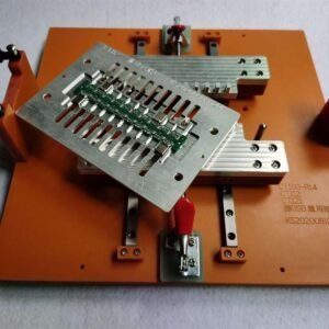
The first bottleneck appeared during manual soldering of the USB connector.
Positioning the PCB and connector required considerable care. The operation involved repeated adjustments, making it difficult to maintain an efficient and repeatable workflow.
Adding operators was not our first choice. Instead, our engineering team examined whether the process could be simplified through better positioning and dedicated tooling.
We developed a dedicated soldering fixture to help position the PCB and USB connector more consistently and reduce unnecessary handling during the operation.
Process change: a dedicated fixture was introduced to support positioning and reduce repeated manual adjustments. No quantified throughput improvement is claimed here.
This process change illustrates the role of tooling in an assembly operation. Connector accessibility, positioning accuracy, and fixture requirements all deserve consideration when preparing a PCB assembly for manufacturing.
These are practical considerations in PCBA assembly, particularly when a design moves beyond prototype builds and into higher-volume production.
2. PCB Functional Testing: Investigating Contact Alignment
The soldering fixture change did not remove the need to investigate the separate testing process.
The next challenge appeared during PCB functional testing.
The test fixture used spring-loaded probes, commonly known as pogo pins, to contact designated test points on the PCB. During operation, the probes did not consistently align with their corresponding contacts, making the testing process difficult to run efficiently.
Assembly and testing need to be reviewed together. A tooling change at one operation does not, by itself, establish the capacity of the production line.
For manufacturers preparing to scale production, it is important to evaluate the capacity of the entire process rather than focusing on the speed of a single assembly operation.
3. Investigating PCB Test Fixture Alignment and Contact Reliability
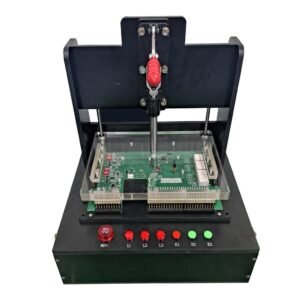
Our engineering and process engineering (PE) teams went to the production line to investigate the testing issue.
The immediate concern was the alignment between the fixture’s spring-loaded probes and the designated PCB contacts. Reliable electrical contact depends on appropriate probe positioning, fixture alignment, and repeatable positioning of the board.
After examining the setup, the team adjusted the probe positioning to address the contact alignment problem.
The investigation also identified a further improvement opportunity: making the relevant test points more accessible through an external test-point arrangement.
This was proposed as a way to simplify test contact positioning and potentially improve testing efficiency. It should be distinguished from the probe-positioning adjustment already carried out.
A verified post-adjustment testing throughput figure was not available for this case study. We therefore do not claim that the testing bottleneck was fully resolved or that the line subsequently achieved the customer’s target output.
The experience reinforced an important consideration in PCB testing and inspection: testing performance depends not only on the test equipment, but also on test-point accessibility, fixture design, probe positioning, and reliable electrical contact.
4. Applying DFM and DFT Before PCBA Mass Production
Looking back at the project, both bottlenecks highlight the value of considering manufacturing and testing requirements before a product enters mass production.
For USB connector soldering, the relevant questions include:
- Can the connector be positioned and soldered consistently?
- Does the assembly process provide sufficient access for the operator and tooling?
- Would a dedicated fixture improve repeatability and reduce unnecessary handling?
For PCB functional testing, the questions are different:
- Can the test probes reliably reach the designated test points?
- Does the fixture maintain appropriate alignment with the PCB?
- Are the test points accessible enough to support repeatable electrical contact?
- Has the testing process been evaluated against the required production volume?
These considerations are closely related to Design for Manufacturability (DFM) and Design for Testability (DFT).
DFM focuses on making a product easier and more consistent to manufacture. DFT considers how a product can be tested effectively and reliably. Applying both principles early can help engineering teams identify potential assembly and testing challenges before they disrupt production.
For additional industry information and technical resources, engineers can consult IPC, an organization that develops standards and resources for the electronics manufacturing industry.
For new projects, Vosnor’s engineering and NPI support considers assembly feasibility, tooling requirements, test access, and manufacturing preparation as part of the transition toward production.
The objective is to identify foreseeable manufacturing challenges early, when design or process changes may be easier to implement.
5. Key Lessons from This PCBA Manufacturing Case Study
This PCBA manufacturing case study highlights two distinct production challenges and the engineering work undertaken to investigate them.
- Assembly tooling matters. A dedicated soldering fixture was introduced to support positioning during USB connector assembly.
- Testing requires reliable contact. Probe alignment was identified as an issue during PCB functional testing, and the team adjusted the probe positioning.
- Further improvements need verification. An external test-point arrangement was identified as an additional improvement opportunity, but a verified post-adjustment testing throughput figure was not available.
- Production capacity must be evaluated as a whole. A faster assembly operation does not automatically resolve a separate testing constraint.
For companies moving from prototype to volume production, the lesson is straightforward:
A working prototype demonstrates that a design can function. It does not, by itself, demonstrate that the product can be manufactured and tested consistently at the required production volume.
Vosnor works with customers to consider practical manufacturing requirements alongside product functionality.
From SMT and THT assembly to functional testing and production preparation, the focus extends beyond whether a board works to how it can be assembled, tested, and prepared for production.
Planning Your Next PCBA Project?
If you are developing a new electronic product or preparing an existing design for volume production, reviewing assembly and testing requirements early can help your team identify potential manufacturing constraints.
Discuss your design, production targets, and engineering requirements with the Vosnor Engineering Team to explore the appropriate next steps for your PCBA project.
PCBA Manufacturing · Engineering Support · PCB Testing · Prototype to Volume Production